affiliate marketing electrolabzz: avr
Showing posts with label avr. Show all posts

Monday, 7 January 2013

Electromagnetic Floater


Electromagnetic Floater


This will show you how to make a device that can float almost any object with a magnet in it.

It is much like the floating globes you can buy, except it works by balancing the forces of permanent magnets with electromagnets, rather then simply using combinations of permanent magnets.
This is done by using a microcontroller and an IR sensor to detect where an object is floating below. Then based on a set value, the microcontroller uses the electromagnets to to hold the floating object at a given height.

The place the object floats at depends on the weight of the object and the power of the magnets in the object. The height is set by holding the object under the magnets and sensor and pushing the button.
The object floats at the point where the force of gravity down equals the force of the magnets pulling up, which allows it to use non-industrial electromagnets and less power to float. The program also dynamically adjusts so the object is always at the perfect height. 
Electromagnetic Floater


Step 1Materials


Materials:
- ATMega168 Microcontroller
- 1 16-20 MHz Crystal
- 28 Pin Socket
- Dual Full H Bridge IC
- 1 Power NPN
- 2 Electromagnets
- 1 Bicolour LED
- 2 IR LED
- 1 IR Photodiode
- 1 5V Regulator
- 2 Leveling Capacitors
- 1 SPST Switch
- 1 NO Button
- 1, 470 Ohm Resistor
- 1, 5 Ohm Resistor
- 1 Universal Breadboard
- 2 Cases
- Plexiglas
- Solder
- Hot Glue
- Steel Wire
- Vinyl Tubing
- 3 or more 1/4" diameter x 1/4" thick rare earth magnets (for the base)
- 2 or more 1/2" diameter x 1/8" thick rare earth magnets (for the objects)

Tools:
- Soldering Iron
- Hot Glue Gun
- Desoldering Pump
- 3rd Hand
- Plexiglas cutter


Step 2Prepare The Base


Prepare The Base

Prepare The Base

Step 3Install the Magnets and Sensor


Install the Magnets and Sensor

Install the Magnets and Sensor


Step 4Build the circuit


Build the Electronics

Build the Electronics

Build the Electronics

Build the Electronics


Step 5   program the device

The hex code of the project is here


Step 6  Test it


Start Floating

Start Floating

Start Floating


DON!!!!!!          


USB programmer for Atmel AVR controllers


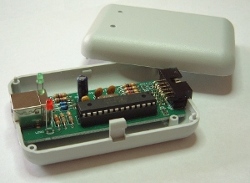
USBasp Foto

USBasp is a USB in-circuit programmer for Atmel AVR controllers. It simply consists of an ATMega88 or an ATMega8 and a couple of passive components. The programmer uses a firmware-only USB driver, no special USB controller is needed.

Features

  • Works under multiple platforms. Linux, Mac OS X and Windows are tested.
  • No special controllers or smd components are needed.
  • Programming speed is up to 5kBytes/sec.
  • SCK option to support targets with low clock speed (< 1,5MHz).
  • Planned: serial interface to target (e.g. for debugging).

Download

Firmware and circuit

The following packages include circuit and firmware.
usbasp.2011-05-28.tar.gz (519 kB) TPI support (upcoming release of avrdude will use it), supports programmers with ATMega88 and ATMega8.
usbasp.2009-02-28.tar.gz (260 kB)
usbasp.2007-10-23.tar.gz (172 kB)
usbasp.2007-07-23.tar.gz (176 kB)
usbasp.2006-12-29.tar.gz (118 kB) Supports programmers with ATMega48 and ATMega8.
usbasp.2006-09-16.tar.gz (116 kB) New VID/PID!
usbasp.2005-11-14.tar.gz (175 kB)
usbasp.2005-07-03.tar.gz (166 kB)
usbasp.2005-04-21.tar.gz (169 kB)

Please refer to Readme.txt for details on building, installing and using USBasp.

Drivers

On Linux and MacOS X no kernel driver is needed. Windows requires a driver for USBasp:
usbasp-windriver.2011-05-28.zip (70 kB)

Software

Hardware

Schematic


please post your comments

Simple Analog to Digital Converter


Normally analogue-to-digital con-verter (ADC) needs interfacing through a microprocessor to convert analogue data into digital format. This requires hardware and necessary software, resulting in increased complexity and hence the total cost.
The circuit of A-to-D converter shown here is configured around ADC 0808, avoiding the use of a microprocessor. The ADC 0808 is an 8-bit A-to-D converter, having data lines D0-D7. It works on the principle of successive approximation. It has a total of eight analogue input channels, out of which any one can be selected using address lines A, B and C. Here, in this case, input channel IN0 is selected by grounding A, B and C address lines.
Usually the control signals EOC (end of conversion), SC (start conversion), ALE (address latch enable) and OE (output enable) are interfaced by means of a microprocessor. However, the circuit shown here is built to operate in its continuous mode without using any microprocessor. Therefore the input control signals ALE and OE, being active-high, are tied to Vcc (+5 volts). The input control signal SC, being active-low, initiates start of conversion at falling edge of the pulse, whereas the output signal EOC becomes high after completion of digitisation. This EOC output is coupled to SC input, where falling edge of EOC output acts as SC input to direct the ADC to start the conversion.
As the conversion starts, EOC signal goes high. At next clock pulse EOC output again goes low, and hence SC is enabled to start the next conversion. Thus, it provides continuous 8-bit digital output corresponding to instantaneous value of analogue input. The maximum level of analogue input voltage should be appropriately scaled down below positive reference (+5V) level.
The ADC 0808 IC requires clock signal of typically 550 kHz, which can be easily derived from an astable multivibrator constructed using 7404 inverter gates. In order to visualise the digital output, the row of eight LEDs (LED1 through LED8) have been used, wherein each LED is connected to respective data lines D0 through D7. Since ADC works in the continuous mode, it displays digital output as soon as analogue input is applied. The decimal equivalent digital 
output value D for a given analogue input voltage Vin can be calculated from the relationship


Saturday, 5 January 2013

Quantum computer

A quantum computer is any device for computation that makes direct use of distinctively quantum mechanical phenomena, such as superposition and entanglement, to perform operations on data.

n a classical (or conventional) computer, information is stored as bits; in a quantum computer, it is stored as qubits (quantum bits).
The basic principle of quantum computation is that the quantum properties can be used to represent and structure data, and that quantum mechanisms can be devised and built to perform operations with this data. Although quantum computing is still in its infancy, experiments have been carried out in which quantum computational operations were executed on a very small number of qubits.
Research in both theoretical and practical areas continues at a frantic pace, and many national government and military funding agencies support quantum computing research to develop quantum computers for both civilian and national security purposes, such as cryptanalysis. If large-scale quantum computers can be built, they will be able to solve certain problems exponentially faster than any of our current classical computers (for example Shor's algorithm).
Quantum computers are different from other computers such as DNA computers and traditional computers based on transistors.
Some computing architectures such as optical computers may use classical superposition of electromagnetic waves, but without some specifically quantum mechanical resources such as entanglement, they have less potential for computational speed-up than quantum computers. The power of quantum computers Integer factorization is believed to be computationally infeasible with an ordinary computer for large integers that are the product of only a few prime numbers (e.g., products of two 300-digit primes).
By comparison, a quantum computer could solve this problem more efficiently than a classical computer using Shor's algorithm to find its factors.
This ability would allow a quantum computer to "break" many of the cryptographic systems in use today, in the sense that there would be a polynomial time (in the number of bits of the integer) algorithm for solving the problem.
In particular, most of the popular public key ciphers are based on the difficulty of factoring integers, including forms of RSA.
These are used to protect secure Web pages, encrypted email, and many other types of data.
Breaking these would have significant ramifications for electronic privacy and security.
The only way to increase the security of an algorithm like RSA would be to increase the key size and hope that an adversary does not have the resources to build and use a powerful enough quantum computer.
It seems plausible that it will always be possible to build classical computers that have more bits than the number of qubits in the largest quantum computer.
For more information about the topic Quantum computer, read the full article at Wikipedia.org, or see the following related articles:

Microbes: New Genetic Fingerprint Lives in Your Gut

A new study suggests that the collection of microbial DNA in the gut is just as individualized as our own human DNA. (Credit: U.S. Department of Agriculture/Washington University)


Our bodies contain far more microbial genes than human genes. And a new study suggests that just as human DNA varies from person to person, so too does the massive collection of microbial DNA in the intestine.


The research is the first to catalog the genetic variation of microbes that live in the gut, where they extract nutrients from food, synthesize vitamins, protect against infections, and produce compounds that naturally reduce inflammation. The widespread genetic diversity uncovered by the scientists can help them understand how our microbial genes work together with our human genes to keep us healthy or, in some cases, to cause disease.
The study, by researchers at Washington University School of Medicine in St. Louis and the European Molecular Biology Laboratory in Heidelberg, Germany, is published online Dec. 5 in Nature.
"Surprisingly, each of us can be identified by the collective DNA of our gut microbes," says corresponding author George Weinstock, PhD, associate director of The Genome Institute at Washington University."That collection is individualized, completely analogous to our human genome. Differences in the way individuals respond to various drugs or the way they use specific nutrients can be traced to the genetic variation in our microbial genes as well as in our human genes."
The researchers analyzed the microbial DNA in 252 stool samples from 207 individuals living in the United States and Europe. All the subjects had participated in one of two recent high-profile initiatives to catalog the diverse species of microbes that live in and on the body. Neither of those studies -- the Human Microbiome Project, funded by the National Institutes of Health, and the Metagenomics of the Human Intestinal Tract (MetaHIT) project, funded by the European Commission -- looked at the genetic variation of the microbial genomes in the body.
For the new study, the researchers zeroed in on 101 species of microbes commonly found in the intestine, identifying more than 10 million single-letter changes in the collective DNA of those microbes. They also found numerous other DNA alterations, including insertions, deletions and structural changes.
In 43 subjects for whom the researchers had two stool samples collected at least a month apart (most were collected six months to a year after the initial sample), the researchers found very little variability in the microbial DNA over time, although the species of microbes in the intestine fluctuated.
"The microbial DNA in the intestine is remarkably stable, like a fingerprint," Weinstock explains. "Even after a year, we could still distinguish individuals by the genetic signature of their microbial DNA."
Babies become colonized with microbes as they pass through the birth canal and into the world. Those microbes come from their mothers and from the environment. Exactly how the microbes shape our lives is not yet known, but in the gut research has suggested that an imbalance of bacteria may contribute to irritable bowel syndrome, Crohn's and even obesity.
With this new catalog, the researchers can begin to understand the selective forces that shape the microbiome -- the collection of microbes and their genes -- in the intestine.
"The DNA of our microbes is a historical record of the microbial evolution in our bodies," says co-author Makendonka Mitreva, PhD, assistant professor of medicine. "Many of these organisms would have colonized us when we were very young and would have grown and evolved with us throughout our lifetimes."
The information gleaned from future studies of the gut microbiome also may help scientists determine how the microbial genes can be manipulated to improve human health and the effectiveness of certain medications, she adds.
Story Source:
The above story is reprinted from materials provided byWashington University in St. Louis. The original article was written by Caroline Arbanas.

Nanotech Device Mimics Dog's Nose to Detect Explosives

Portable, accurate, and highly sensitive devices that sniff out vapors from explosives and other substances could become as commonplace as smoke detectors in public places, thanks to researchers at University of California, Santa Barbara.


Concept illustration of the microscale free-surface microfluidic channel as it concentrates vapor molecules that bind to nanoparticles inside a chamber. A laser beam detects the nanoparticles, which amplify a spectral signature of the detected molecules. (Credit: Image courtesy of University of California - Santa Barbara)


Researchers at UCSB, led by professors Carl Meinhart of mechanical engineering and Martin Moskovits of chemistry, have designed a detector that uses microfluidic nanotechnology to mimic the biological mechanism behind canine scent receptors. The device is both highly sensitive to trace amounts of certain vapor molecules, and able to tell a specific substance apart from similar molecules.
"Dogs are still the gold standard for scent detection of explosives. But like a person, a dog can have a good day or a bad day, get tired or distracted," said Meinhart. "We have developed a device with the same or better sensitivity as a dog's nose that feeds into a computer to report exactly what kind of molecule it's detecting." The key to their technology, explained Meinhart, is in the merging of principles from mechanical engineering and chemistry in a collaboration made possible by UCSB's Institute for Collaborative Biotechnologies.
Results published this month inAnalytical Chemistry show that their device can detect airborne molecules of a chemical called 2,4-dinitrotoluene, the primary vapor emanating from TNT-based explosives. The human nose cannot detect such minute amounts of a substance, but "sniffer" dogs have long been used to track these types of molecules. Their technology is inspired by the biological design and microscale size of the canine olfactory mucus layer, which absorbs and then concentrates airborne molecules.
"The device is capable of real-time detection and identification of certain types of molecules at concentrations of 1 ppb or below. Its specificity and sensitivity are unparalleled," said Dr. Brian Piorek, former mechanical engineering doctoral student in Meinhart's laboratory and Chief Scientist at Santa Barbara-based SpectraFluidics, Inc . The technology has been patented and exclusively licensed to SpectraFluidics, a company that Piorek co-founded in 2008 with private investors.
"Our research project not only brings different disciplines together to develop something new, but it also creates jobs for the local community and hopefully benefits society in general," commented Meinhart.
Packaged on a fingerprint-sized silicon microchip and fabricated at UCSB's state-of-the-art cleanroom facility, the underlying technology combines free-surface microfluidics and surface-enhanced Raman spectroscopy (SERS) to capture and identify molecules. A microscale channel of liquid absorbs and concentrates the molecules by up to six orders of magnitude. Once the vapor molecules are absorbed into the microchannel, they interact with nanoparticles that amplify their spectral signature when excited by laser light. A computer database of spectral signatures identifies what kind of molecule has been captured.
"The device consists of two parts," explained Moskovits. "There's a microchannel, which is like a tiny river that we use to trap the molecules and present them to the other part, a mini spectrometer powered by a laser that detects them. These microchannels are twenty times smaller than the thickness of a human hair."
"The technology could be used to detect a very wide variety of molecules," said Meinhart. "The applications could extend to certain disease diagnosis or narcotics detection, to name a few."
Moskovits added, "The paper we published focused on explosives, but it doesn't have to be explosives. It could detect molecules from someone's breath that may indicate disease, for example, or food that has spoiled."
The fundamental research was developed through an interdisciplinary collaboration between Professors Meinhart and Moskovits, and carried out by former doctoral researchers Dr. Piorek and Dr. Seung-Joon Lee. Their project was funded in part by UCSB's Institute for Collaborative Biotechnologies through the Army Research Office and DARPA.

Story Source:
The above story is reprinted from materials provided byUniversity of California - Santa Barbara.

Progress for Spintronics: Spin Amplifier Works at Room Temperature

 A fundamental cornerstone for spintronics that has been missing up until now has been constructed by a team of physicists at Linköping University in Sweden. It's thought to be the world's first spin amplifier that can be used at room temperature.
A schematic picture of the defect-engineered spin amplifier demonstrated in this work. The wave pattern symbolizes the time variation of the spin signal, namely the difference between the numbers of spin-up and spin-down electrons. The red and blue arrows represent the period with more spin-up and spin-down electrons, respectively. The amplitude of the wave reflects the strength of the spin signal, which is weak before entering the spin amplifier but becomes stronger when exiting. The defects that have enabled the spin-amplification functionality of a non-magnetic semiconductor are indicated by the yellow balls, each with a spin-polarized localized electron (indicated by the red and blue arrows). The spin direction of this localized electron rapidly follows the sign of the input spin signal, which serves to only attract and remove the incoming electrons with an undesired spin orientation. This leads to a significant enhancement in the spin polarization of the electrons passing the spin amplifier, giving rise to a strongly amplified output spin signal that has truthfully cloned the exactly same time-varying function and thus the spin-encoded information of the input spin signal. (Credit: Weimin Chen/Adv. Mater. 2012, DOI 10.1002/adma.20120597)


Great hopes have been placed on spintronics as the next big paradigm shift in the field of electronics. Spintronics combines microelectronics, which is built on the charge of electrons, with the magnetism that originates in the electrons' spin. This lays the foundation for entirely new applications that fire the imagination. The word "spin" aims at describing how electrons spin around, much like how Earth spins on its own axis.
But turning theory into practice requires amplifying these very weak signals. Instead of transistors, rectifiers, and so on, the building blocks of spintronics will be formed by things like spin filters, spin amplifiers, and spin detectors. Through regulating and controlling electron spin, it will be possible to store data more densely and process it many times faster -- and with greater energy efficiency -- than today's technology.
In 2009, an LiU group from the Department of Functional Electronic Material, led by Professor Weimin Chen, presented a new type of spin filter that works at room temperature. The filter lets through electrons that have the desired spin direction, screening out the others. This function is crucial for constructing new types of components such as spin diodes and spin lasers.
Now the same group, in collaboration with colleagues from Germany and the United States, has published an article in the highly-ranked journal Advanced Materials, where they present an effective spin amplifier based on a non-magnetic semiconductor. The amplification occurs through deliberate defects in the form of extra gallium atoms introduced into an alloy of gallium, indium, nitrogen and arsenic.
A component of this kind can be set anywhere along a path of spin transport to amplify signals that have weakened along the way. By combining this with a spin detector, it may be possible to read even extremely weak spin signals.
"It's an advance that blazes a trail for a solution to the problem of controlling and detecting electron spin at room temperature, which is a prerequisite for the breakthrough of spintronics," says Weimin Chen.
Story Source:
The above story is reprinted from materials provided byLinköping University, via EurekAlert!, a service of AAAS.

On-Demand Synaptic Electronics: Circuits That Learn and Forget

Researchers in Japan and the US propose a nanoionic device with a range of neuromorphic and electrical multifunctions that may allow the fabrication of on-demand configurable circuits, analog memories and digital-neural fused networks in one device architecture.


(a): Volatile (short-term) memory property of two terminal Pt/WO3-x/Pt device before the forming process. Current change observed by applying sequence of positive voltage pulses at intervals of 40 s and widths of 0.5 s. Read voltage was 0.5 V. (b): Non-volatile (long-term) memory property in the device after forming process following application of sequence of positive and negative pulses with widths of 0.1 ms. Read voltage was 0.1 V. (c): Schematic illustration of the device structures before and after forming process. (Credit: Image courtesy of International Center for Materials Nanoarchitectonics (MANA))

Synaptic devices that mimic the learning and memory processes in living organisms are attracting avid interest as an alternative to standard computing elements that may help extend Moore's law beyond current physical limits.
However so far artificial synaptic systems have been hampered by complex fabrication requirements and limitations in the learning and memory functions they mimic. Now Rui Yang, Kazuya Terabe and colleagues at the National Institute for Materials Science in Japan and the University of California, Los Angeles, in the US have developed two-, three-terminal WO3-x-based nanoionic devices capable of a broad range of neuromorphic and electrical functions.
In its initial pristine condition the system has very high resistance values. Sweeping both negative and positive voltages across the system decreases this resistance nonlinearly, but it soon returns to its original state indicating a volatile state. Applying either positive or negative pulses at the top electrode introduces a soft-breakdown, after which sweeping both negative and positive voltages leads to non-volatile states that exhibit bipolar resistance and rectification for longer periods of time.
The researchers draw similarities between the device properties -- volatile and non-volatile states and the current fading process following positive voltage pulses -- with models for neural behaviour -- that is, short- and long-term memory and forgetting processes. They explain the behaviour as the result of oxygen ions migrating within the device in response to the voltage sweeps. Accumulation of the oxygen ions at the electrode leads to Schottky-like potential barriers and the resulting changes in resistance and rectifying characteristics. The stable bipolar switching behaviour at the Pt/WO3-x interface is attributed to the formation of the electric conductive filament and oxygen absorbability of the Pt electrode.
As the researchers conclude, "These capabilities open a new avenue for circuits, analog memories, and artificially fused digital neural networks using on-demand programming by input pulse polarity, magnitude, and repetition history."

Story Source:
The above story is reprinted from materials provided byInternational Center for Materials Nanoarchitectonics (MANA), via ResearchSEA.

Sensor Detects Bombs On Sea Floor


Scientists have developed a sensor to detect undetonated explosives on the sea floor, based on a technology used to find mineral deposits underground.

The sensor was developed as part of a project with US Government agency, the Strategic Environmental Research and Development Program (SERDP) and US-based research organisation Sky Research.
The method for finding undetonated underwater explosives is very similar to that used to detect underground mineral deposits, says CSIRO electrical engineer Dr Keith Leslie.
“Our highly sensitive sensor – the high temperature superconducting tensor gradiometer – delivers significantly more information about the target’s magnetic field than conventional sensors used for this type of detection,” he said.
“It provides data on the location, characterisation and magnetic qualities of a target – whether it is a gold deposit or an explosive.”
Over 10 million acres of coastal waters are contaminated by undetonated explosives, according to SERDP. Typically these small explosives rust and corrode at sea, making them even more dangerous.
“The marine environment is difficult to sample due to electrical currents produced by waves, which affect underwater magnetic fields,” Dr Leslie said.
“In mineral exploration, near surface deposits are being exhausted, leading our search for minerals deeper underground, where targets are more difficult to detect with traditional surface and airborne measurements.”
Our sensor can provide valuable geological information that discriminates between prospective and non-prospective areas or targets. It avoids unnecessary drilling and minimises the risk of overlooking valuable mineral deposits.
“Our sensor has a critical advantage for small targets such as undetonated explosives, where only one or two measurements may be near the target,” Dr Leslie said.
“In mineral exploration, a string of measurements of the gradients of the magnetic field down a drill hole can determine the direction to the target.”
Eventually the technology may renew exploration efforts at abandoned sites where drilling programs were based on insufficient or inaccurate information. It also has the potential to help clear landmines.
The sensor has been proved in a stationary laboratory environment. Trials have been conducted to prove it in motion, in preparation for anticipated underwater trials.
Story Source:
The above story is reprinted from materials provided byCSIRO Australia.

Artificial Intelligence Helps Sort Used Batteries

 Research at the University of Gothenburg, Sweden and Chalmers University of Technology, Sweden has resulted in a new type of machine that sorts used batteries by means of artificial intelligence (AI). One machine is now being used in the UK, sorting one-third of the country's recycled batteries.

'I got the idea at home when I was sorting rubbish. I thought it should be possible to do it automatically with artificial intelligence,' says Claes Strannegård, who is an AI researcher at the University of Gothenburg and Chalmers University of Technology.
Strannegård contacted the publically owned recycling company Renova in Gothenburg, Sweden, who were positive to an R&D project concerning automatic sorting of collected batteries. The collaboration resulted in a machine that uses computerised optical recognition to sort up to ten batteries per second.
The sorting is made possible by the machine's so-called neural network, which can be thought of as an artificial nervous system. Just like a human brain, the neural network must be trained to do what it is supposed to do. In this case, the machine has been trained to recognise about 2,000 different types of batteries by taking pictures of them from all possible angles.
As the batteries are fed into the machine via a conveyor belt, they are 'visually inspected' by the machine via a camera. The neural network identifies the batteries in just a few milliseconds by comparing the picture taken with pictures taken earlier. The network is self-learning and robust, making it possible to recognise batteries even if they are dirty or damaged. Once the batteries have been identified, compressed air separates them into different containers according to chemical content, such as nickel-cadmium or lithium.
'For each single battery, the system stores and spits out information about for example brand, model and type. This allows the recycler to tell a larger market exactly what types of material it can offer, which we believe may increase the value through increased competition,' says Hans-Eric Melin, CEO of the Gothenburg-based company Optisort, which has developed the machine.
This means that besides the environmental benefits of the machine, there are commercial benefits. Today the collection and sorting companies are actually paying money to get rid of the batteries. But Melin thinks that real-time battery data could spark a new market for battery waste, where large volumes are traded online.
So far, the company has delivered two machines -- one to Renova in Gothenburg (where half of all the batteries collected in Sweden are sorted) and one to G&P Batteries in the UK. The interest in Optisort and its machine is rising and Strannegård, who founded the company, is very happy his idea is turning out to work so well in the real world.
'This is sparking further research and development so that we will eventually use artificial intelligence to sort all types of waste,' he says.


Story Source:
The above story is reprinted from materials provided byUniversity of Gothenburg. The original article was written by Thomas Melin.

Liquid Metal Used to Create Wires That Stretch Eight Times Their Original Length

Researchers from North Carolina 
State University have created conductive wires that can be stretched up to eight times their original length while still functioning. The wires can be used for everything from headphones to phone chargers, and hold potential for use in electronic textiles.
The tube, filled with liquid metal, can be stretched many times its original length. (Credit: Image courtesy of North Carolina State University)

To make the wires, researchers start with a thin tube made of an extremely elastic polymer and then fill the tube with a liquid metal alloy of gallium and indium, which is an efficient conductor of electricity.
"Previous efforts to create stretchable wires focus on embedding metals or other electrical conductors in elastic polymers, but that creates a trade-off," says Dr. Michael Dickey, an assistant professor of chemical and biomolecular engineering at NC State and co-author of a paper on the research.
"Increasing the amount of metal improves the conductivity of the composite, but diminishes its elasticity," Dickey says. "Our approach keeps the materials separate, so you have maximum conductivity without impairing elasticity. In short, our wires are orders of magnitude more stretchable than the most conductive wires, and at least an order of magnitude more conductive than the most stretchable wires currently in the literature."
While the manufacturing of the new wires is relatively straightforward, Dickey notes that one challenge needs to be addressed before the wires can be considered for popular products: how to minimize leakage of the metal if the wires are severed.
The paper, "Ultrastretchable Fibers with Metallic Conductivity Using a Liquid Metal Alloy Core," is published online inAdvanced Functional Materials. The paper was co-authored by Shu Zhu, a former undergraduate at NC State; Dr. Ju-Hee So, a former Ph.D. student at NC State; Robin Mays and William Barnes, Ph.D. students at NC State; Dr. Sharvil Desai, a former postdoctoral researcher at NC State; and Dr. Behnam Pourdeyhimi, the William A. Klopman Distinguished Chaired Professor of Materials in NC State's College of Textiles and a professor of chemical and biomolecular engineering in the university's College of Engineering.
The research was funded by a National Science Foundation (NSF) CAREER award and the NSF's Research Triangle Materials Research Science & Engineering Center.

Data Storage: A Fast and Loose Approach Improves Memory

An unconventional design for a nanoscale memory device uses a freely moving mechanical shuttle to improve performance.

A loose and rattling part in your cell phone is generally a cause for concern. Like most other electronic devices, your phone works by moving electrons through fixed circuit pathways. If electrons are not sufficiently contained within these pathways, the efficiency and speed of a device decrease. However, as the miniature components inside electronic devices shrink with each generation, electrons become harder to contain. Now, a research team led by Vincent Pott at the A*STAR Institute of Microelectronics, Singapore, has designed a memory device using a loose and moving part that actually enhances performance.
The loose part is a tiny metal disk, or shuttle, about 300 nanometers thick and 2 micrometers long, and lies inside a roughly cylindrical metal cage. Because the shuttle is so small, gravity has little effect on it. Instead, the forces of adhesion between the shuttle and its metal cage determine its position. When stuck to the top of its cage, the shuttle completes an electrical circuit between two electrodes, causing current to flow. When it is at the bottom of the cage, the circuit is broken and no current flows. The shuttle can be moved from top to bottom by applying a voltage to a third electrode, known as a gate, underneath the cage.
Pott and co-workers suggested using this binary positioning to encode digital information. They predicted that the forces of adhesion would keep the shuttle in place even when the power is off, allowing the memory device to retain information for long periods of time. In fact, the researchers found that high temperature -- one of the classic causes of electronic memory loss -- should actually increase the duration of data retention by softening the metal that makes up the shuttle memory's disk and cage, thereby strengthening adhesion. The ability to operate in hot environments is a key requirement for military and aerospace applications.
The untethered shuttle also takes up less area than other designs and is not expected to suffer from mechanical fatigue because it avoids the use of components that need to bend or flex -- such as the cantilevers used in competing mechanical memory approaches. In a simulation, Pott and co-workers found that the shuttle memory should be able to switch at speeds in excess of 1 megahertz.
The next steps, the researchers say, include designing arrays of the devices and analyzing fabrication parameters in detail. If all goes well, their novel device could compete head-to-head with the industry-standard FLASH memory.
The A*STAR-affiliated researchers contributing to this research are from the Institute of Microelectronics/

Physicists Take Photonic Topological Insulators to the Next Level

Researchers at The University of Texas at Austin have designed a simulation that for the first time emulates key properties of electronic topological insulators.


Their simulation, which was described this week in Nature Materials, is part of a rapidly moving scientific race to understand and exploit the potential of topological insulators, which are a state of matter that was only discovered in the past decade. These insulators may enable dramatic advances in quantum computing and spintronics.
"The discovery of these materials, which are insulators in their volume while capable of conducting current on their surface, was a bit of a surprise to the condensed matter community," said Gennady Shvets, professor of physics in the College of Natural Sciences. "Before that, we classified solid materials into three categories, based on their ability to conduct electric current: insulators, conductors, and semiconductors. Topological insulators fall somewhere in between."
Shvets co-authored the article with his physics department colleagues Alexander Khanikaev, S. Hossein Mousavi, Wang-Kong Tse, Mehdi Kargarian, and Professor Allan MacDonald.
He said that what's particularly exciting about topological insulators is that they can conduct electrons -- or in the case of photonic ones, photons -- in a way that protects them from scattering or reflecting when they encounter obstacles.
"Usually when photons run into an obstacle, they reflect," said Shvets. "We are basically designing interfaces in such a way that they lock photons into one spin state. So in one direction they're in one spin state, and when they're going in another direction they're locked into another spin state. In that configuration they cannot reflect without changing their spin, which is forbidden by the design of the photonic crystal. They flow around defects and can be routed along arbitrarily shaped paths defined by the interface."
If this property could be achieved with electrons it would be particularly relevant to quantum computers, which are likely to require their electrons to maintain coherence for a much longer time than digital computers.
Over the past decade scientists have had modest success making or finding electronic topological insulators. But these substances are limited both in what they can do and in what they can reveal about the potential of this new state of matter.
"Those systems are very difficult to study systematically, because when you have a real material it is what it is. You're limited to studying its properties," said Shvets. "Nature doesn't give you the knobs to increase or decrease various aspects of it, so it's very difficult to benchmark the existing theories against what's observed."
Shvets and his physics department colleagues expect that their simulated photonic insulator will be a much more powerful and flexible tool for studying the general properties of topological insulators.
"With these purely artificial photonic crystals, we can study these systems in a more systematic way," he said.
In order for their insights from the photonic system to be applicable to electronic systems, Shvets and his colleagues had to make their simulated photons behave sufficiently like electrons. To do that, they designed simulated "metamaterials." These are artificial electromagnetic materials that can be tuned to influence photons in ways that are otherwise impossible. Other metamaterials are being used to develop invisibility cloaks.
Shvets and his colleagues designed what they've called SPINDOMs (spin-degenerate optically-active metamaterials). When arranged periodically, the resulting meta-crystals are the first demonstration that it's possible to control the spin of photons in a way that emulates what can be done with electrons.
This is significant on a few fronts. Even as a computer simulation it allows researchers to explore the properties of topological insulators. When these photonic topological insulators are physically built, as Shvets and his colleagues hope will be done soon, they'll allow more exploration. And there's great promise that such insulators may eventually be used to reduce interference in wireless communications systems.
"Right now if you put multiple emitting or receiving antennas in close proximity to each other, whether on a semiconductor chip or on top of a cellular base station, the radiation from each antenna is affected by the others," he said. "To deal with this you have to design around it. What would be better is if all cross talk between emitting/receiving sources could just be eliminated. That's what we believe could be done by photonic topological insulators, which can directionally guide electromagnetic waves."

Spintronics: Producing AC Voltages by Manipulating Magnetic Fields

Scientists are putting a new spin on their approach to generating electrical current by harnessing a recently identified electromotive force known as spinmotive force, which is related to the field of spintronics that addresses such challenges as improving data storage in computers. Now, a novel application of spintronics is the highly efficient and direct conversion of magnetic energy to electric voltage by using magnetic nanostructures and manipulating the dynamics of magnetization.


According to a report published in the American Institute of Physics' (AIP) journal Applied Physics Letters, this conversion could be the foundation for future development of spin-based power electronics, a field the authors call "power spintronics." Their newly published results of an experimental model suggest that a power spintronics-based device may one day be a promising approach to obtaining alternating current (AC) voltages from direct current (DC) magnetic fields.
The researchers demonstrated for the first time the feasibility of a device that generates a voltage based on manipulating an effective magnetic field within a nanowire that arises from width modulation. Technically such a field is not a true magnetic field, but it can be viewed as such. The team tested a one-dimensional model. It showed that DC magnetic field characteristics such as magnitude, and design parameters such as wire width, can be used to control, or "tune," the frequency and amplitude of AC current. Importantly, their results showed that a variable frequency ranging from megahertz to gigahertz can be achieved. Control and range in tuning ability are highly desirable management features in generating current.
The team's results suggest that applying their spintronics approach may one day meet a variety of commercial energy demands due to control and scalability.

New Energy-Efficient Computer Memory Using Magnetic Materials

By using electric voltage instead of a flowing electric current, researchers from UCLA's Henry Samueli School of Engineering and Applied Science have made major improvements to an ultra-fast, high-capacity class of computer memory known as magnetoresistive random access memory, or MRAM.

Add caption

MeRAM bit. (Credit: Image courtesy of University of California - Los Angeles)


The UCLA team's improved memory, which they call MeRAM for magnetoelectric random access memory, has great potential to be used in future memory chips for almost all electronic applications, including smart-phones, tablets, computers and microprocessors, as well as for data storage, like the solid-state disks used in computers and large data centers.
MeRAM's key advantage over existing technologies is that it combines extraordinary low energy with very high density, high-speed reading and writing times, and non-volatility -- the ability to retain data when no power is applied, similar to hard disk drives and flash memory sticks, but MeRAM is much faster.
Currently, magnetic memory is based on a technology called spin-transfer torque (STT), which uses the magnetic property of electrons -- referred to as spin -- in addition to their charge. STT utilizes an electric current to move electrons to write data into the memory.
Yet while STT is superior in many respects to competing memory technologies, its electric current-based write mechanism still requires a certain amount of power, which means that it generates heat when data is written into it. In addition, its memory capacity is limited by how close to each other bits of data can be physically placed, a process which itself is limited by the currents required to write information. The low bit capacity, in turn, translates into a relatively large cost per bit, limiting STT's range of applications.
With MeRAM, the UCLA team has replaced STT's electric current with voltage to write data into the memory. This eliminates the need to move large numbers of electrons through wires and instead uses voltage -- the difference in electrical potential -- to switch the magnetic bits and write information into the memory. This has resulted in computer memory that generates much less heat, making it 10 to 1,000 times more energy-efficient. And the memory can be more than five-times as dense, with more bits of information stored in the same physical area, which also brings down the cost per bit.
The research team was led by principal investigator Kang L. Wang, UCLA's Raytheon Professor of Electrical Engineering, and included lead author Juan G. Alzate, an electrical engineering graduate student, and Pedram Khalili, a research associate in electrical engineering and project manager for the UCLA-DARPA research programs in non-volatile logic.
"The ability to switch nanoscale magnets using voltages is an exciting and fast-growing area of research in magnetism," Khalili said. "This work presents new insights into questions such as how to control the switching direction using voltage pulses, how to ensure that devices will work without needing external magnetic fields, and how to integrate them into high-density memory arrays.
"Once developed into a product," he added, "MeRAM's advantage over competing technologies will not be limited to its lower power dissipation, but equally importantly, it may allow for extremely dense MRAM. This can open up new application areas where low cost and high capacity are the main constraints."
Said Alzate: "The recent announcement of the first commercial chips for STT-RAM also opens the door for MeRAM, since our devices share a very similar set of materials and fabrication processes, maintaining compatibility with the current logic circuit technology of STT-RAM while alleviating the constrains on power and density."
The research was presented Dec. 12 in a paper called "Voltage-Induced Switching of Nanoscale Magnetic Tunnel Junctions" at the 2012 IEEE International Electron Devices Meeting in San Francisco, the semiconductor industry's "pre-eminent forum for reporting technological breakthroughs in the areas of semiconductor and electronic device technology."
MeRAM uses nanoscale structures called voltage-controlled magnet-insulator junctions, which have several layers stacked on top of each other, including two composed of magnetic materials. However, while one layer's magnetic direction is fixed, the other can be manipulated via an electric field. The devices are specially designed to be sensitive to electric fields. When the electric field is applied, it results in voltage -- a difference in electric potential between the two magnetic layers. This voltage accumulates or depletes the electrons at the surface of these layers, writing bits of information into the memory.
"Ultra-low-power spintronic devices such as this one have potential implications beyond the memory industry," Wang said. They can enable new instant-on electronic systems, where memory is integrated with logic and computing, thereby completely eliminating standby power and greatly enhancing their functionality."
The work was supported by the Defense Advanced Research Projects Agency (DARPA) NV Logic Program. Other authors included researchers from the UCLA Department of Electrical Engineering; UC Irvine's Department of Physics and Astronomy; Hitachi Global Storage Technologies (a Western Digital Company); and Singulus Technologies, of Germany.

Technology Allows Scientists to Capture and Preserve Cancer Cells Circulating in the Bloodstream

Scientists from the RIKEN Advanced Science Institute in Japan and University of California Los Angeles report a new nanoscale Velcro-like device that captures and releases tumor cells that have broken away from primary tumors and are circulating in the bloodstream.This new nanotechnology could be used for cancer diagnosis and give insight into the mechanisms of how cancer spreads throughout the body. The device provides a convenient and non-invasive alternative to biopsy, the current method for diagnosis of metastatic cancer


A new-generation nano-platform capable of capturing circulating tumor cells and releasing them at reduced temperature. (Credit: RIKEN)


It could enable doctors to detect tumor cells that circulate in cancer patients' blood well before they subsequently colonize as tumors in other organs. The device also enables researchers to keep the tumor cells alive and subsequently study them.
The device was developed by a team led by Hsiao-hua Yu from the RIKEN Advanced Science Institute in Japan and Hsian-Rong Tseng from the Department of Molecular and Medical Pharmacology at the University of California Los Angeles, in research published online December 17 in the journal Advanced Materials.
Similar cell-capture devices have been reported but this technology is unique in that it is capable of catching the tumor cells with great efficiency and releasing them with great cell viability. Blood is passed through the device like a filter that contains a molecule capable of adhering to tumor cells like Velcro and separating them with efficiency ranging from 40% to 70%. The cancer cells are retained by tiny temperature-responsive polymer brushes inside the device. At 37 degrees Celsius, these polymer brushes stick to the tumor cells, but when cooled to 4 degrees Celsius, they release them, allowing scientists to examine the cells.
"Until now, most devices have demonstrated the ability to capture circulating tumor cells with high efficiency. However, it is equally important to release these captured cells, to preserve and study them in order to obtain insightful information about them. This is the big difference with our device." Explains Hsiao-hua Yu, who led the team that developed the technique to coat the device with polymer brushes.